
Industry Outlook Report
April 2025
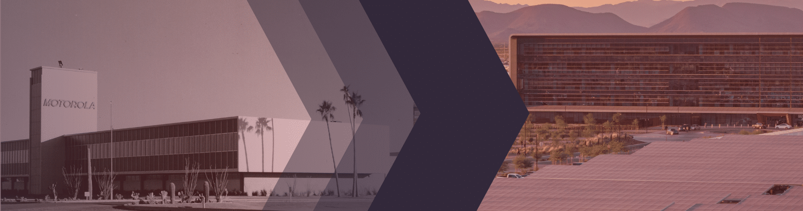
From a single Motorola research lab in 1949 to Taiwan Semiconductor Manufacturing Company’s (TSMC) ongoing investments in its multi-fab, 1,100-acre manufacturing campus, Greater Phoenix’s semiconductor industry1 growth strategy has primed the region to mature into one of the most vertically integrated hubs in the nation — and by extension, the world.
The numbers speak for themselves: data from the Semiconductor Industry Association (SIA) shows that Greater Phoenix’s end-to-end semiconductor value chain has garnered the most investment of any U.S. metro since 2020: over $100 billion.2 In early 2025, Greater Phoenix Economic Council (GPEC) convened local semiconductor leaders and experts at roundtable events to assess the industry’s current state and discuss what might be coming next. These conversations contributed to many of the insights contained in this report.
No. 1
Metro for Semiconductor Supply Chain Investment Since 2020
33K+
Semiconductor Industry Jobs3
No. 4
Largest Semiconductor Industry Workforce in the Nation4
Major Employers
| Company | Description | Greater Phoenix Employees |
|---|---|---|
|
Operates four fabs in Chandler, with two more leading-edge fabs under construction |
12,000+ |
|
One of six planned fabs in Phoenix is operational, and construction is complete on the second; an in-state research and development (R&D) center and two advanced packaging facilities were recently confirmed |
3,000+ |
|
Operates two fabs in Chandler, producing semiconductor products that serve the automotive, advanced telecom and defense markets |
1,000+ |
|
Designer of microcontrollers and memory products; maintains corporate headquarters (HQ) in Chandler |
1,000+ |
|
Designer and manufacturer of semiconductor wafer processing equipment, with North American HQ in the region since the 1970s and new HQ, R&D and operations center planned in Scottsdale |
1,000 |
|
Developer of power/signal management devices as well as discrete and logic products; has corporate HQ and R&D center in Scottsdale |
600+ |


Source: MAG 2023 Employer Database; TSMC, ASM and onsemi internal estimates
Growth & Trends
| 2024 Metric | Regional Context | 5-Year Local Industry Growth Trend | 5-Year National Industry Growth Trend | |
|---|---|---|---|---|
Employment |
33,598 |
1.4% of regional jobs |
13.8% |
7.3% |
Payrolled Business Locations |
666 |
0.5% of payrolled business locations |
10.6% |
11.4% |
Average Earnings per Job |
$174,091 |
208% higher than average earnings for all industries |
14.7% |
22.3% |
Gross Regional Product (GRP) |
$10.6 billion |
2.9% of total GRP |
29.7% |
24.9% |
Source: Lightcast 2025 Q1
Emerging Opportunities
Artificial Intelligence
The chip industry has been manufacturing products that have altered global markets and geopolitics for three-quarters of a century. This dynamic continues today. The dizzying pace of advancement in artificial intelligence (AI) — a technology which is precipitating tectonic shifts in business practices and labor markets, almost in real-time — relies on advanced semiconductors. In particular, the high arithmetic throughput and low latency afforded by leading-edge chips have been crucial to train and run large language models.
Greater Phoenix is no stranger to the externalities of technological progress enabled by semiconductors, such as automation. Case in point: while the region’s semiconductor industry today has roughly as many jobs as it did in 2007, it is 40% more productive.5 Today, Greater Phoenix’s leading role within the global semiconductor landscape means it will contribute to shaping our world’s technological future for years to come. TSMC’s site in north Phoenix is currently the only location in the U.S. where 4nm logic chips are manufactured, and the firm is ramping up 3nm production schedules in response to AI demand from customers. At full build-out, TSMC expects 30% of its 2nm and more advanced production to be located in Arizona. Announced customers for its Arizona-made chips include AMD, Apple and NVIDIA. It will soon be joined by Intel’s Fab 52 and 62 in Chandler, the former of which will produce 1.8nm, leading-edge wafers.
Supplier Spotlight
Although fabs tend to garner the headlines, they are significantly outnumbered by the expansive network of semiconductor suppliers, service and equipment providers, and sales offices that have moved to Greater Phoenix in their wake. Since 2021, GPEC has helped attract nearly 40 of these companies to the market, which together will occupy 5 million square feet of real estate, employ nearly 3,900 people, and invest more than $3 billion in their local operations. Notable ecosystem members who recently opened or announced new operations in Greater Phoenix include:
Tokyo Electron
Semiconductor production equipment manufacturer with sales office in Chandler
DSV
Specialty logistics provider with multiple locations across Greater Phoenix
Chang Chun Arizona
Chemical manufacturing plant in Casa Grande
Pentagon Technologies
Cleaning, coating and contamination services at two locations in Greater Phoenix
Applied Materials
Semiconductor equipment manufacturer with $270 million R&D facility co-located with Arizona State University (ASU) in Tempe
Of course, the semiconductor ecosystem comprises more than simply the newest logic chips (see “Supplier Spotlight” above). The release of DeepSeek in early 2025 showed that there may be a future for AI models that rely on less advanced chips. While high-performance computing should continue to outperform the rest of the semiconductor space in the near term, demand for data centers (a sector which is expected to see between 8% and 11% compound annual growth through 2030; robust for a mature industry) coupled with the demand potentially induced by new AI models may lead to increased business across the breadth of the semiconductor value chain. Given the vertical diversity of the region’s semiconductor landscape — it is the only U.S. metro to receive substantial investments across all ecosystem categories tracked by SIA since 2020 — Greater Phoenix may stand to benefit regardless of which market segment ultimately drives demand.
Advanced Packaging
The need for chip miniaturization in medical devices, telecommunications, autonomous and electric vehicles, and AI is expected to bolster the advanced packaging market over the next decade as fabs run up against the limits of Moore’s Law (the observation that R&D progress doubles the number of transistors on microchips every two years or so). However, overproduction issues and softening demand in certain sectors led to a weak 2024 for advanced packaging. Even so, the development of advanced wafer-scale packaging and three-dimensional (3D) chip stacking for high-performance applications is underway, and Greater Phoenix has positioned itself to mature into a nexus of advanced packaging commercial activity and R&D. Amkor, currently a market leader in 3D advanced packaging, is building in the city of Peoria what should be the largest outsourced advanced packaging and testing facility in the U.S. ASU and Tempe-based Deca Technologies are also leading a $100 million R&D effort funded by the Department of Commerce’s National Advanced Packaging Manufacturing Program. The third and final flagship CHIPS for America R&D facility, which will be located in ASU’s Research Park in the city of Tempe, will focus in part on advanced packaging research. Additionally, in April of 2025 TSMC announced that its two new advanced packaging facilities will be located in Arizona.
Photonics
The heat and speed efficiencies of silicon photonics technology possess considerable potential for the next generation of semiconductors. Arizona enjoys homegrown strengths in photonics and the broader optics industry, both in industry and academic R&D, to such an extent that the state’s southeastern region (centered on the Tucson metro) has earned the nickname “Optics Valley”. The University of Arizona in Tucson is home to the Wyant College of Optical Sciences, a world-class research center in optics and photonics with an extensive Industrial Affiliate program that includes the likes of ASML, Edmund Optics, and Apple, among many others. In Greater Phoenix, ASU operates the Advanced Electronics and Photonics Core Facility, a state-of-the-art lab whose recent research portfolio includes improvements in photosensitive semiconductor design. While the Tucson region remains the state’s optics and photonics innovation hub, Greater Phoenix is often the location where optics innovations are applied and scaled6 — an important ecosystem role in its own right.
De-risking
Many types of knowledge work have grown place-agnostic since the pandemic, but high-tech manufacturing has shown an enduring preference for clusters and supplier/buyer co-location. Greater Phoenix’s status as a semiconductor hub has contributed to the growth of several productive industry clusters that use chips as inputs, including automobiles, medical devices and aerospace and defense. The latter of these is of heightened importance as the U.S. looks to minimize security risks in a shifting, uncertain global environment. To this end, the Southwest Advanced Prototyping (SWAP) Hub, headed by ASU, is one of only eight regional innovation hubs established by the Department of Defense Microelectronics Commons to mitigate the nation’s dependence on microelectronics from foreign and adversarial countries. The SWAP Hub drives research and product prototyping/testing/development with a focus on high trust supply chains and production, the challenges posed by space and extreme environments, and industry-informed microelectronics workforce development. Access to unmatched R&D facilities — including the ASU MacroTechnology Works building in Tempe — offer startups the opportunity to prove their technology before investing in expensive capital equipment.
From a geopolitical perspective, several members of GPEC’s Industry Roundtable believe that proximity and cost-effectiveness might make Mexico a beneficiary of the semiconductor industry’s near- and friend-shoring efforts. Arizona may be well-served by maintaining its efforts to collaborate with Mexican states with attested manufacturing capabilities, such as Sonora and Baja California, as global supply chains are reconfigured. For example, ASU (with funding from the U.S. Department of State) is partnering with the government of Mexico and several other allies across the western hemisphere and Asia to accelerate near-shoring opportunities in the semiconductor assembly, testing and packaging subindustry.
Strategies Driving Future Success
Energy Infrastructure
A preliminary investigation of internal GPEC data indicates that electrical power requirements for the average industrial user considering relocating or expanding to the region may have doubled between fiscal years 2021 and 2024. Semiconductor firms and their suppliers are one of the clearly identifiable sectors driving this growth. Aligning regional utilities’ energy portfolios and generation strategies with the intensive needs of future users is of the utmost importance for the next stage of the semiconductor industry in Greater Phoenix, as the capital costs and lead times that spiked during the pandemic are only increasing, and once-infrequent requests for bespoke onsite generation setups from firms looking to go operational as fast as possible are becoming more common.
Achieving this alignment will require a top-to-bottom reassessment of the interdependent policies governing the grid. Though not every potential reform will be adopted, and solutions will differ from region to region, a holistic suite of multijurisdictional reforms should be on the table: from targeted reassessments of the approval processes and transmission restrictions governed by the National Environmental Protection Act and the Federal Energy Regulatory Commission at the federal level, to the consideration of microgrid strategies, small and medium nuclear reactors and portfolio diversification at the state and utility level, to reducing permitting times at the municipal level.
Semiconductors and Water
The high water requirements of the semiconductor industry are well publicized. Equally worthy of attention are the lengths to which Arizona chipmakers have gone to radically reduce water consumption, pursuing innovative engineering solutions not always seen in other domestic semiconductor manufacturing markets, like zero or near-zero liquid discharge. Intel, which has cultivated a long and productive water conservation partnership with the city of Chandler, achieved net water positivity at its Arizona fabs in 2022 and restored 1.1 billion gallons of water to the state in 2023. For its part, TSMC is on pace to recycle 65% of the water used at its first fab. The recycling rate should jump to 90% when its recycling facility comes online in 2027.

1.1B Gallons of Water Restored to the State in 2023 by Intel
65% of Used Water will be Recycled at TSMC’s First Fab, with a Projected Increase to 90% by 2027
Workforce Development and Top Talent Attraction
Greater Phoenix has made significant semiconductor workforce gains in recent years, netting over 4,000 new jobs since 2020.7 The future looks bright as well: the region ranked first among all domestic metros in semiconductor ecosystem jobs expected from post-2020 investments stimulated by the CHIPS & Science Act, with over 13,000 jobs announced.8 Several local leaders at GPEC’s Industry Roundtables spoke highly of the engineering talent coming out of educational institutions like ASU and Grand Canyon University, and others praised ongoing workforce development collaborations with the region’s community colleges.
Still, some talent gaps persist. Despite its diverse ecosystem base and impressive job growth, Greater Phoenix is not a major player in the high-end fabless chip design that has fueled the AI revolution. The most sought-after talent in this space remains concentrated in San Jose, California. Relatedly, some local leaders stressed the continued difficulty of attracting this type of top-tier, PhD-level talent and plan to continue time- and capital-intensive strategies like talent circulation, whereby highly skilled employees are relocated to Arizona from as far away as Southeast Asia to fill vital roles within the organization, while junior Arizona talent is sent to out of state or international headquarters to undergo training. Some employers also stress pain points around hiring the right entry-level semiconductor processing technicians, though the responsive local workforce programming stemming from cooperation between industry and education systems mentioned above has helped.
Momentum in Innovation
Because the capital required for technological advancement in the semiconductor industry is so substantial, the intellectual property protections afforded by patents are key risk mitigators in assuring returns on investment. In addition to its well-earned reputation as a semiconductor manufacturing center, Greater Phoenix is also a major source of semiconductor intellectual property talent. In 2022 Greater Phoenix surpassed the Albany, New York metro as the third most productive region for unique semiconductor patent filings by individual local inventors, and now sits behind only San Jose, California and Portland, Oregon.
Unique Semiconductor Patent Filings by Local Inventors
| Metro | 2024 | Average Annual Filing Growth, 2018-24 |
|---|---|---|
San Jose, CA |
3,413 |
-3.3% |
Portland, OR |
2,077 |
11.6% |
Phoenix, AZ |
1,245 |
7.5% |
Albany, NY |
1,012 |
-16.1% |
San Francisco, CA |
864 |
-7.3% |
Source: U.S. Patent and Trademark Office. “Data Download Tables.” PatentsView. Accessed March 2025. Data excludes December 2024
The region’s chip R&D momentum extends beyond recent patent filings and into the near future — Greater Phoenix ranks third among all US metros in CHIPS R&D Program awards9 and will likely vault to first with the early 2025 announcement of a multibillion Chips for America R&D Flagship Facility led by Natcast (the operator of the National Semiconductor Technology Center) in ASU’s Research Park. Firm-level strategic decisions are also contributing: ASM, a multinational Dutch company which designs and produces semiconductor wafer processing equipment, has planned its largest R&D facility worldwide in Scottsdale, while power and sensing device manufacturer onsemi unveiled its corporate HQ and Design and Solution Engineering Center in Scottsdale in 2023. TSMC confirmed in 2025 that it will site a new R&D center in Arizona to complement its six fabs and two advanced packaging facilities, with the goal of completing its AI supply chain in the U.S. The state and region must encourage this recent run of success in cultivating innovation assets to round out wins in attracting manufacturing operations. If the center of gravity for the AI industry continues its shift towards Arizona, this might entail partnerships or the outright expansion of innovation targets such as leading-edge fabless design (mentioned above) or electronic design automation firms. Long-term targets could include hyperscalers such as Apple, Amazon and Meta that have been moving semiconductor design increasingly in-house and making production co-investments.
Download the PDF on the Future of Semiconductors in Greater Phoenix.

Report Author
Kevin Carranza
Vice President, Research & Analytics

Industry Expert
Sean Fogarty
Vice President, International Business Development
1. The definition of the “semiconductor/chip industry” in this report comprises the following NAICS codes: 333242, 334412, 334413, 334416, 334417, 334418, 334419, 334515 and 423690. The term “semiconductor ecosystem” includes the semiconductor industry plus businesses in a variety of industries that supply and transact with it. 2. Semiconductor Industry Association. (2025, March 7). Semiconductor Supply Chain Investments. 3. Lightcast 2025 Q1 4. Lightcast 2025 Q1 5. Lightcast 2025 Q1 6. Arizona Commerce Authority. (2023, March 1). How Arizona established itself as a leader in advanced optics. American City Business Journals. 7. Lightcast 2025 Q1 8. Semiconductor Industry Association. (2025, March 7). Semiconductor Supply Chain Investments. 9. Semiconductor Industry Association. (2025, March 12). CHIPS R&D Programs. https://www.semiconductors.org/chips-rd-programs/
Published: 04/22/2025